Research Bio
Ali Javey is the Lam Research Distinguished Chair in Semiconductor Processing and a professor of Electrical Engineering and Computer Sciences. The core of Javey’s research program is materials innovation for enabling new device structures and concepts. The lab studies a wide range of electronic materials in both planar and 3D geometries. In all cases, the lab explores new schemes of manipulating, processing, and engineering materials - often at unprecedented levels - to enable new functionalities and properties. Below are some research highlights.
- Developed a new doping technology named monolayer doping (MLD) that utilizes surface chemistry to form self-assembled monolayers of dopant containing species on semiconductor surfaces followed by a subsequent diffusion by a thermal annealing (Nature Materials, 2008). The process has yielded some of the shallowest junctions reported to date, down to ~3 nm in thickness. The technology has been transferred to the semiconductor industry for further internal R&D, and is seen as a promising approach for S/D contact extensions for future nanoscale transistors.
- Developed the ultrathin body III-V on insulator (XOI) device concept as a platform for integrating high mobility III-V semiconductors on Si for low power electronics (Nature, 2010). Reported p- and n-type III-V FETs with some of the highest mobilities reported to-date on a Si substrate with a subthreshold swing as low as ~70 mV/decade, approaching the ideal limit of MOSFETs.
- Discovered the quantum unit of absorptance in 2D semiconductors (in collaboration with E. Yablonovitch; PNAS, 2013).
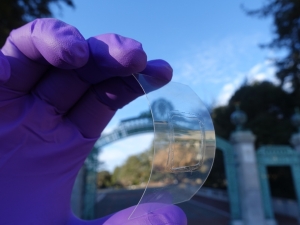
- Developed a new growth mode for III-V thin films using the vapor-liquid-solid (VLS) technique (Scientific Reports, 2013). As a proof of concept, InP thin films (on the order of 1µm in thickness) are grown on non-epitaxial substrates (e.g., metal foils) using the thin-film VLS process with an ultralarge grain size of up to ~ 1mm and optoelectronic properties (including luminescence yield) approaching those of epitaxially grown layers. The work presents a promising route for low-cost growth of high quality III-V semiconductors for PV applications and beyond.
- Developed process techniques for uniform assembly of nanostructured materials (e.g., nanowires and nanotubes) over large-areas for system integration – moving beyond individual device work (Nature Materials, 2013; Nature Materials, 2010). As a proof of concept, Javey’s lab has demonstrated large-area monolithic integration of nanotube TFTs, pressure sensors, and OLEDs on a plastic substrate that can map pressure and provide instantaneous visual response through the integrated OLED display. The work presents a platform for 3-D integration of different material/device components for paper-thin smart/interactive surfaces, and is an elegant example of systems enabled by nanomanufacturing.
Research Expertise and Interest
nanotechnology, low power electronics, flexible electronics and sensors, nanofabrication, energy harvesting and conversion, programmable matter
In the News

The Nose Knows: Electric Schnoz Can Smell When Your Food’s Gone Bad

Don’t Sweat It!
LED Material Shines Under Strain
Researchers demonstrate new semiconductor device possibilities using black phosphorous
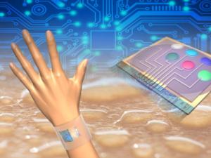
Wearable sensors detect what’s in your sweat
Atomically thin light emitting device opens the possibility for ‘invisible’ displays
Physiological Changes Tracked Moment to Moment
Smallest. Transistor. Ever.
Let them see you sweat: What new wearable sensors can reveal from perspiration
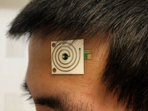
A new sensor developed at UC Berkeley can be made into “smart” wristbands or headbands that provide continuous, real-time analysis of the chemicals in sweat.
Berkeley Researchers Develop Highly Sensitive Tactile Sensors for Robotics and Other Applications
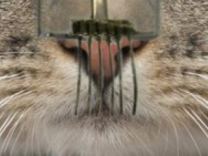
From the world of nanotechnology we’ve gotten electronic skin, or e-skin, and electronic eye implants or e-eyes. Now we’re on the verge of electronic whiskers.
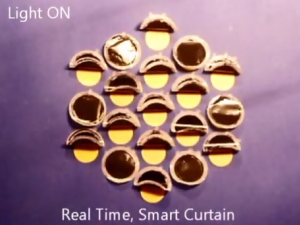
Research Brief: Engineers create light-activated ‘curtains’
Forget remote-controlled curtains. A new development by researchers at the University of California, Berkeley, could lead to curtains and other materials that move in response to light, no batteries needed.
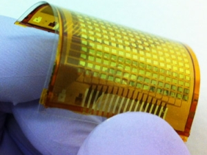
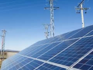
Research Brief: Technology could bring high-end solar to the masses
Engineers at the University of California, Berkeley, have developed an inexpensive new way to grow thin films of a material prized in the semiconductor and photovoltaic industries, an achievement that could bring high-end solar cells within reach of consumer pocketbooks.
Paper-thin e-skin responds to touch, holds promise for sensory robotics and interactive environments
A new milestone by engineers at UC Berkeley can help robots become more touchy-feely, literally.
UC Berkeley's Ali Javey Winner of APEC Science Prize for Innovation Research and Education
U.S. Secretary of Energy Steven Chu awarded the 2011 APEC Science Prize to UC Berkeley Professor Ali Javey in San Francisco today. Professor Javey is well known for developing low-cost, flexible, and lightweight photovoltaic cells. He has also developed transistor arrays that use a fraction of the power of conventional silicon transistors.
DOE awards $25 million to UC Berkeley, Stanford to lower cost of solar power
The effort to make sun power more affordable has gotten a big boost with a $25 million, five-year Department of Energy grant announced this week. The award launches the Bay Area Photovoltaics Consortium (BAPVC), led jointly by the University of California, Berkeley, and Stanford University.
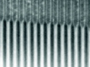
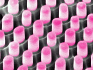
A New Twist for Nanopillar Light Collectors
UC Berkeley researchers have created unique dual-diameter nanopillars – narrow at the top, broad at the bottom – that absorb light as well or even better than commercial thin-film solar cells, using far less semiconductor material and without the need for anti-reflective coating.
Engineers make artificial skin out of nanowires
UC Berkeley engineers have developed a pressure-sensitive electronic material from semiconductor nanowires that could one day be used as an artificial skin for robots and prosthetic limbs.
Researcher Ali Javey, still shy of 30, is a nano scientist with big aspirations
Working at the confluence of electrical engineering and materials science, chemistry and physics, Associate Professor Ali Javey, 29, has already collected an armload of accolades and achieved several research breakthroughs, including a novel method for nanowire printing.
Teaching
Individual Study or Research [AST 299 - 014]
Microfabrication Technology [ELENG 143 - 001]
Individual Study or Research [AST 299 - 025]
Integrated-Circuit Devices [ELENG 130 - 001]
Integrated-Circuit Devices [ELENG 230A - 001]
Individual Study or Research [AST 299 - 014]
Integrated-Circuit Devices [ELENG 130 - 001]
Integrated-Circuit Devices [ELENG 230A - 001]