New Microscope Technology Energizes Undergraduate Research

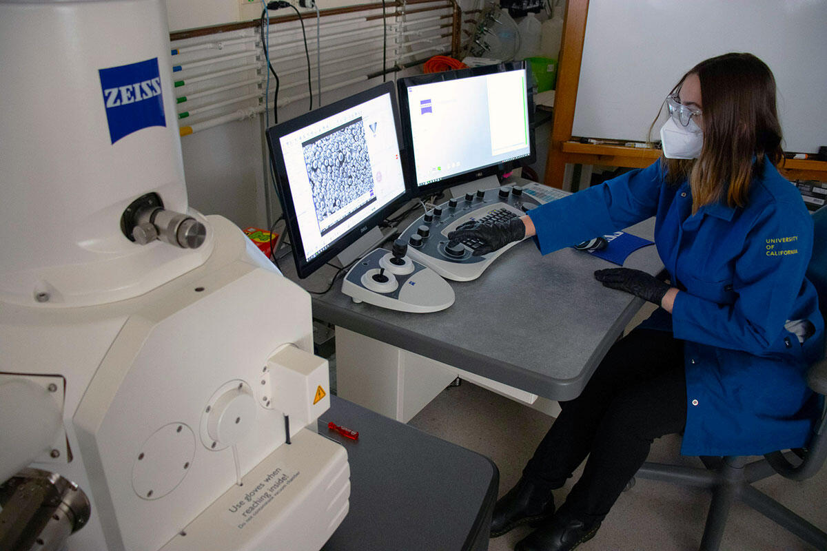
The College of Chemistry has received a new state-of-the-art EVO LS 15 scanning electron microscope (SEM) provided by ZEISS in support of the instructional physical chemistry labs. The new SEM will allow our students to take images of nanoscale matter down to 3 nm spatial resolution. In doing so, ZEISS is supporting our educational and research mission to train undergraduates with modern technology relevant to chemistry and nanoscience to help prepare them for the job market after their studies at UC Berkeley.
This support of our hands on instructional approach allows us to enable lab experiments for students who are interested in conducting research at the vibrant interface of chemistry, materials science, and nanoscience. It is important for the College to use modern technology to train our students and provide them with the opportunity to experience top-of-the-line instrumentation they would find, for example, if they later started their professional careers in the semiconductor industry.
There are two ways the instrument is being implemented in our instructional and research activities. First, we have integrated the instrument into our upper division physical chemistry lab courses where students can learn about the technology and applications, with the opportunity to perform hands-on quantitative material analysis. Second, both undergraduate and graduate students can perform their independent and group experiments using the instrument to inspect research samples. This ability to capture real-space images at the nanoscale of samples that students prepare by chemical synthesis, enables bringing together different areas of their training in a unique way, namely the relationship between materials processing and characterization.
Key aspects of this microscope are the high spatial resolution and ease of operation so that students who have never seen an SEM before can effectively walk into the lab and take pictures of their samples with nanoscale resolution after only a brief training session. Michael Zuerch, assistant professor of chemistry, who oversaw the SEM's installation and is training the students on the new machine states, “It reminds me of my time when I did an SEM lab experiment myself as a student perhaps 15 years ago. I spent a whole afternoon doing alignments and then taking a few poorly resolved images on a much older SEM. That our students can now so easily take sharp images in a short period of time and focus on their chemical and materials system under study rather than instrument optimization, shows how much this technology has advanced.”
The computer-controlled instrument interface will also allow for students to participate remotely in lab experiments through screen sharing. Throughout this partnership between the College and ZEISS, the student experiences in the classroom, with hands-on instruction, will in turn benefit development of the next generation of these instruments through feedback to the product and applications teams at ZEISS.
Senior Nadia Berndt discusses her experience with the new scanning electron microscope (SEM)
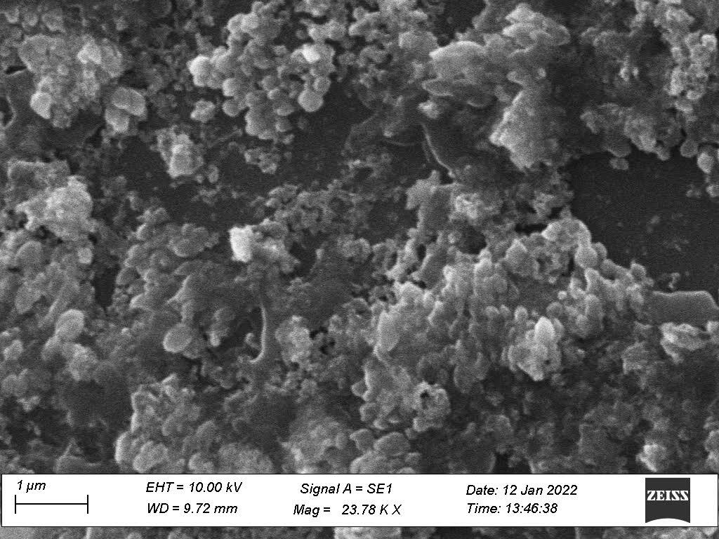
In her research project this semester, Nadia Berndt is investigating charge dynamics in clay encapsulated 2D materials to understand why the addition of the clay increases the photocatalytic abilities of these materials. Nadia states, "Previous studies have shown that they form nanoflake structures. By using the SEM I was able to directly visualize the surface of the samples. Below is an example of the surface of one sample. They are quite disorganized, which makes analysis of the dynamics difficult, but not impossible."

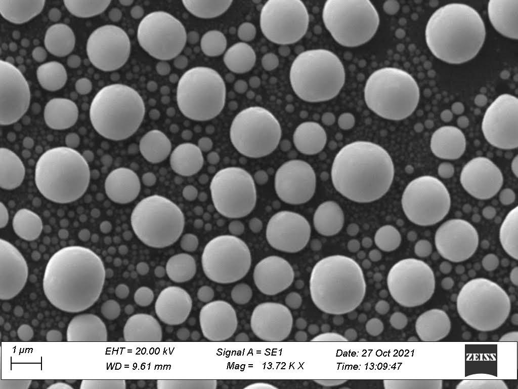
Nadia continues, "The SEM is a great tool for the physical chemistry teaching laboratory as it lets students work with state-of-the-art technology that is used in many related disciplines. Many interesting materials that can be studied. An example is the tin balls in the photo below which gives valuable insights into how structure affects a material's properties. This understanding in turn helps us leverage these relationships so we can develop new materials to solve challenges in our world."

Prof. Zuerch comments, “The new SEM is located in our undergraduate physical chemistry laboratory along with many other cutting-edge instruments. It is being integrated it into our upper-division lab courses in CHEM125 where we expect about 60 to 80 students annually to conduct experiments with the new instrument. In these experiments, students will prepare samples and use the SEM to conduct the experiments that allow them to quantify size distributions of crystals that are synthetically grown under varying conditions.”
About ZEISS
ZEISS Research Microscopy Solutions(link is external) is the world's only one-stop manufacturer of light, electron, X-ray and ion microscope systems and offers solutions for correlative microscopy. The portfolio is comprised of products and services for life sciences, materials and industrial research, as well as education and clinical practice. The unit is headquartered in Jena, Germany. Additional production and development sites are located in Oberkochen, Göttingen and Munich, as well as in Cambridge in the UK, and in Peabody, MA and Pleasanton, CA in the U.S. ZEISS Research Microscopy Solutions is part of the Industrial Quality & Research segment.
