Engineers take plasmon lasers out of deep freeze
Researchers at the University of California, Berkeley, have developed a new technique that allows plasmon lasers to operate at room temperature, overcoming a major barrier to practical utilization of the technology.
The achievement, described Dec. 19 in an advanced online publication of the journal Nature Materials, is a "major step towards applications" for plasmon lasers, said the research team's principal investigator, Xiang Zhang, UC Berkeley professor of mechanical engineering and faculty scientist at Lawrence Berkeley National Laboratory.

"Plasmon lasers can make possible single-molecule biodetectors, photonic circuits and high-speed optical communication systems, but for that to become reality, we needed to find a way to operate them at room temperature," said Zhang, who also directs at UC Berkeley the Center for Scalable and Integrated Nanomanufacturing, established through the National Science Foundation’s (NSF) Nano-scale Science and Engineering Centers program.
In recent years, scientists have turned to plasmon lasers, which work by coupling electromagnetic waves with the electrons that oscillate at the surface of metals to squeeze light into nanoscale spaces far past its natural diffraction limit of half a wavelength. Last year, Zhang's team reported a plasmon laser that generated visible light in a space only 5 nanometers wide, or about the size of a single protein molecule.
But efforts to exploit such advancements for commercial devices had hit a wall of ice.
"To operate properly, plasmon lasers need to be sealed in a vacuum chamber cooled to cryogenic temperatures as low as 10 kelvins, or minus 441 degrees Fahrenheit, so they have not been usable for practical applications," said Renmin Ma, a post-doctoral researcher in Zhang's lab and co-lead author of the Nature Materials paper.
In previous designs, most of the light produced by the laser leaked out, which required researchers to increase amplification of the remaining light energy to sustain the laser operation. To accomplish this amplification, or gain increase, researchers put the materials into a deep freeze.

To plug the light leak, the scientists took inspiration from a whispering gallery, typically an enclosed oval-shaped room located beneath a dome in which sound waves from one side are reflected back to the other. This reflection allows people on opposite sides of the gallery to talk to each other as if they were standing side by side. (Some notable examples of whispering galleries include the U.S. Capitol's Statuary Hall, New York's Grand Central Terminal, and the rotunda at San Francisco's city hall.)
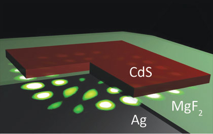
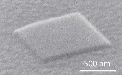
Instead of bouncing back sound waves, the researchers used a total internal reflection technique to bounce surface plasmons back inside a nano-square device. The configuration was made out of a cadmium sulfide square measuring 45 nanometers thick and 1 micrometer long placed on top of a silver surface and separated by a 5 nanometer gap of magnesium fluoride.
The scientists were able to enhance by 18-fold the emission rate of light, and confine the light to a space of about 20 nanometers, or one-twentieth the size of its wavelength. By controlling the loss of radiation, it was no longer necessary to encase the device in a vacuum cooled with liquid helium. The laser functioned at room temperature.
"The greatly enhanced light matter interaction rates means that very weak signals might be observable," said Ma. "Lasers with a mode size of a single protein are a key milestone toward applications in ultra-compact light source in communications and biomedical diagnostics. The present square plasmon cavities not only can serve as compact light sources, but also can be the key components of other functional building-blocks in integrated circuits, such as add-drop filters, direction couplers and modulators."
Rupert Oulton, a former post-doctoral researcher in Zhang's lab and now a lecturer at Imperial College London, is the other co-lead author of the paper. Other co-authors are Volker Sorger, a UC Berkeley Ph.D. student in mechanical engineering, and Guy Bartal, a former research scientist in Zhang's lab.
The U.S. Air Force Office of Scientific Research and the NSF helped support this work.
