Crystal with a twist: scientists grow spiraling new material

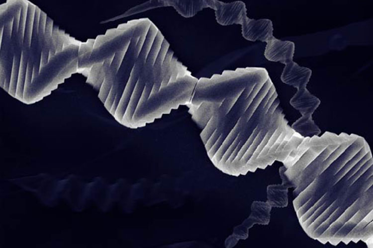
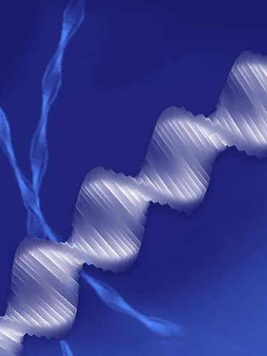
With a simple twist of the fingers, one can create a beautiful spiral from a deck of cards. In the same way, scientists at the University of California, Berkeley, and Lawrence Berkeley National Laboratory (Berkeley Lab) have created new inorganic crystals made of stacks of atomically thin sheets that unexpectedly spiral like a nanoscale card deck.
Their surprising structures, reported in a new study appearing online Wednesday, June 20, in the journal Nature, may yield unique optical, electronic and thermal properties, including superconductivity, the researchers say.
These helical crystals are made of stacked layers of germanium sulfide, a semiconductor material that, like graphene, readily forms sheets that are only a few atoms or even a single atom thick. Such “nanosheets” are usually referred to as “2D materials.”
“No one expected 2D materials to grow in such a way. It’s like a surprise gift,” said Jie Yao, an assistant professor of materials science and engineering at UC Berkeley. “We believe that it may bring great opportunities for materials research.”
While the shape of the crystals may resemble that of DNA, whose helical structure is critical to its job of carrying genetic information, their underlying structure is actually quite different. Unlike “organic” DNA, which is primarily built of familiar atoms like carbon, oxygen and hydrogen, these “inorganic” crystals are built of more far-flung elements of the periodic table — in this case, sulfur and germanium. And while organic molecules often take all sorts of zany shapes, due to unique properties of their primary component, carbon, inorganic molecules tend more toward the straight and narrow.
To create the twisted structures, the team took advantage of a crystal defect called a screw dislocation, a “mistake” in the orderly crystal structure that gives it a bit of a twisting force. This “Eshelby Twist”, named after scientist John D. Eshelby, has been used to create nanowires that spiral like pine trees. But this study is the first time the Eshelby Twist has been used to make crystals built of stacked 2D layers of an atomically thin semiconductor.
“Usually, people hate defects in a material — they want to have a perfect crystal,” said Yao, who also serves as a faculty scientist at Berkeley Lab. “But it turns out that, this time, we have to thank the defects. They allowed us to create a natural twist between the material layers.”

In a major discovery last year, scientists reported that graphene becomes superconductive when two atomically thin sheets of the material are stacked and twisted at what’s called a “magic angle.” While other researchers have succeeded at stacking two layers at a time, the new paper provides a recipe for synthesizing stacked structures that are hundreds of thousands or even millions of layers thick in a continuously twisting fashion.
“We observed the formation of discrete steps in the twisted crystal, which transforms the smoothly twisted crystal to circular staircases, a new phenomenon associated with the Eshelby Twist mechanism,” said Yin Liu, co-first author of the paper and a graduate student in materials science and engineering at UC Berkeley. “It’s quite amazing how interplay of materials could result in many different, beautiful geometries.”
By adjusting the material synthesis conditions and length, the researchers could change the angle between the layers, creating a twisted structure that is tight, like a spring, or loose, like an uncoiled Slinky. And while the research team demonstrated the technique by growing helical crystals of germanium sulfide, it could likely be used to grow layers of other materials that form similar atomically thin layers.
“The twisted structure arises from a competition between stored energy and the energy cost of slipping two material layers relative to one another,” said Daryl Chrzan, chair of the Department of Materials Science and Engineering and senior theorist on the paper. “There is no reason to expect that this competition is limited to germanium sulfide, and similar structures should be possible in other 2D material systems.”
“The twisted behavior of these layered materials, typically with only two layers twisted at different angles, has already showed great potential and attracted a lot of attention from the physics and chemistry communities. Now, it becomes highly intriguing to find out, with all of these twisted layers combined in our new material, if will they show quite different material properties than regular stacking of these materials,” Yao said. “But at this moment, we have very limited understanding of what these properties could be, because this form of material is so new. New opportunities are waiting for us.”
Other co-first authors of the paper include Su Jung Kim and Haoye Sun of UC Berkeley and Jie Wang of Argonne National Laboratory. Other authors include Fuyi Yang, Zixuan Fang, Ruopeng Zhang, Bo Z. Xu, Michael Wang, Shuren Lin, Kyle B. Tom, Yang Deng, Robert O. Ritchie, Andrew M. Minor and Mary C. Scott of UC Berkeley; Nobumichi Tamura, Xiaohui Song, Qin Yu, John Turner and Emory Chan of Berkeley Lab and Jianguo Wen and Dafei Jin of Argonne National Laboratory.
Work at Berkeley Lab’s Molecular Foundry and the Advanced Light Source was supported by the U.S. Department of Energy’s Office of Science and Office of Basic Energy Sciences under contract no. DE-AC02-05CH11231. The research was also supported by the U.S. Department of Energy’s Office of Science, Office of Basic Energy Sciences and Materials Sciences and Engineering Division under contract no. DE-AC02-244 05CH11231 within the Electronic Materials Program (KC1201).
RELATED INFORMATION
