
Research Bio
Michael Crommie is a professor in the Department of Physics. His main research interests lie in exploring the local electronic, magnetic, and mechanical properties of atomic and molecular structures at surfaces. He is interested in studying how local interactions between atomic-scale structures affect their microscopic behavior, and how quantum mechanical effects might influence nanodevice behavior in very small structures. His main experimental tool is scanned probe microscopy, which can be used in combination with other experimental tools to both fabricate atomic-scale structures and probe them spectroscopically.
See current projects.
Research Expertise and Interest
physics, electronic properties of atomic-scale structures at surfaces, atomic-scale structures, morphology and dynamics of mesoscopic systems, atomic manipulation, visualizing low dimensional electronic behavior
In the News
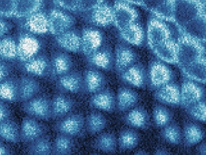
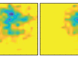
Physicists snap first image of an ‘electron ice’

This Exotic Particle Had an Out-of-Body Experience; These Scientists Took a Picture of It
Graphene ‘camera’ captures real-time electrical activity of beating heart
Metal wires of carbon complete toolbox for carbon-based computers
Tying electrons down with nanoribbons

Bats do it, dolphins do it. Now humans can do it too.
UC Berkeley physicists have used graphene to build lightweight ultrasonic loudspeakers and microphones, enabling people to mimic bats or dolphins’ ability to use sound to communicate and gauge the distance and speed of objects around them.
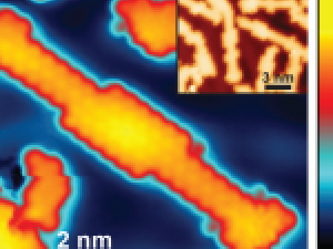
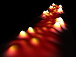
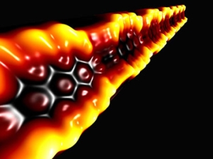
From the Bottom Up: Manipulating Nanoribbons at the Molecular Level
Researchers at Lawrence Berkeley National Laboratory and the University of California, Berkeley, have developed a new precision approach for synthesizing graphene nanoribbons from pre-designed molecular building blocks. Using this process the researchers have built nanoribbons that have enhanced properties—such as position-dependent, tunable bandgaps—that are potentially very useful for next-generation electronic circuitry.
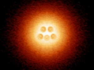
Long Predicted Atomic Collapse State Observed in Graphene
The first experimental observation of a quantum mechanical phenomenon that was predicted nearly 70 years ago holds important implications for the future of graphene-based electronic devices.
Direct Imaging by Berkeley Lab Researchers Confirms the Importance of Electron-Electron Interactions in Graphene
Perhaps no other material is generating as much excitement in the electronics world as graphene. For the vast potential of graphene to be fully realized, however, scientists must first learn more about what makes graphene so super. The latest step in this direction has been taken by researchers with the U.S. Department of Energy (DOE)’s Lawrence Berkeley National Laboratory (Berkeley Lab) and the University of California (UC) Berkeley.
Teaching
Seminars for Graduate Students [CHEM 298 - 021]
Research for Graduate Students [CHEM 299 - 009]
Electromagnetism and Optics [PHYSICS 110A - 002]
Research [PHYSICS 299 - 011]
Individual Study or Research [AST 299 - 008]
Seminars for Graduate Students [CHEM 298 - 073]
Research for Graduate Students [CHEM 299 - 018]
Quantum Mechanics [PHYSICS 137B - 002]
Seminar [PHYSICS 290A - 001]
Research [PHYSICS 299 - 011]
Research [PHYSICS 299 - 001]
Seminars for Graduate Students [CHEM 298 - 021]
Research for Graduate Students [CHEM 299 - 009]
Seminar [PHYSICS 290A - 001]
Research [PHYSICS 299 - 011]
Supervised Research: Physical Sciences [UGIS 192D - 010]