
Research Bio
Andrew Minor is a Professor at the University of California, Berkeley in the Department of Materials Science and Engineering and also holds a joint appointment at the Lawrence Berkeley National Laboratory where he is the Facility Director of the National Center for Electron Microscopy in the Molecular Foundry. He has over 300 publications in the fields of nanomechanics, metallurgy, electron characterization of soft matter and in situ transmission electron microscopy technique development. Minor’s honors include the LBL Materials Science Division Outstanding Performance Award (2006 & 2010), the AIME Robert Lansing Hardy Award from TMS (2012) and the Burton Medal from the Microscopy Society of America (2015). In 2023 he served as the President of the Microscopy Society of America.
Research Expertise and Interest
metallurgy, nanomechanics, electron microscopy, in situ TEM, electron microscopy of soft materials
In the News
Going Cold: The Future of Electron Microscopy
World-Leading Microscopes Take Candid Snapshots of Atoms in Their ‘Neighborhoods’
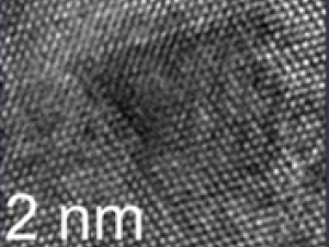
Study Reveals how Oxygen is like Kryptonite to Titanium
UC Berkeley scientists have found the mechanism by which titanium, prized for its high strength-to-weight ratio and natural resistance to corrosion, becomes brittle with just a few extra atoms of oxygen.
Look inside a nano testing machine
Video shows how Berkeley scientists use amazing equipment to develop materials to make future nuclear power plants more reliable and durable.
Testing irradiated materials on the nanoscale
Radiation damages metal and other materials, which can be a problem in nuclear power plants. UC Berkeley/LBNL materials scientist Andrew Minor and colleagues have developed a way to test nano-sized samples to determine how well they withstand the effects of radiation.
Teaching
Seminars for Graduate Students [CHEM 298 - 053]
Research for Graduate Students [CHEM 299 - 029]
Group Studies, Seminars, or Group Research [MATSCI 298 - 016]
Individual Study or Research [MATSCI 299 - 016]
Seminars for Graduate Students [CHEM 298 - 088]
Research for Graduate Students [CHEM 299 - 077]
Group Studies, Seminars, or Group Research [MATSCI 298 - 016]
Individual Study or Research [MATSCI 299 - 016]
Properties of Materials [MATSCI 45 - 001]
Seminars for Graduate Students [CHEM 298 - 053]
Research for Graduate Students [CHEM 299 - 029]
Group Studies, Seminars, or Group Research [MATSCI 298 - 016]
Individual Study or Research [MATSCI 299 - 016]