New chip could lead to cheaper and better medical imaging devices and self-driving cars
Berkeley engineers have created the fastest silicon-based, programmable two-dimensional optical phased array, built on micro-electro-mechanical systems (MEMS). This chip could lead to cheaper and more efficient medical-imaging devices, optical communications and holographic televisions. It could also give rise to more robust light detection and ranging (LiDAR) sensors for self-driving cars. They describe their work in Optica.
The concept of optical phased array has been around for decades, used in applications like medical imaging and optical communications. The idea is to pack an array of light emitters and vary their phase, or the alignment of light waves that they produce. Ultimately, this creates a light source that does not physically move but can project a laser beam in any direction. This kind of agile beamsteering could be useful in LiDAR technology, which determines the distance of nearby objects by sending out laser beams in various directions and measuring how long they take to come back.
Today, the most widely-used LiDAR technology is a rotating box mounted on top of a self-driving vehicle. Known as spinning LiDAR, this technology is expensive to produce and potentially unreliable, as it is not clear whether this moving device can withstand daily use over the course of years. This is why many experts believe that optical phased arrays, known as solid-state LiDAR, is a more promising technology.
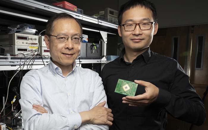
"The biggest challenge for the current optical phased array used in LiDAR is its relative slow beamsteering speed for point-by-point scanning and its limited overall aperture which dominates the system’s optical resolution," said Youmin Wang, a former UC Berkeley postdoctoral researcher and lead author on the paper.
He notes that the spatial light modulators, which modulate the intensity of light beams, in traditional optical phased array designs consist mostly of very small moving parts, so these devices only work in certain wavelengths of light and are limited in the range that they can scan. This limits their efficiency and reliability, as their signals can be affected by surrounding conditions, especially in environments where temperatures change dramatically.
To overcome this limitation, the Berkeley researchers developed a chip that uses MEMS actuators to laterally move a grating element that diffracts light in various directions. This phase-shifting movement adds a delay to outgoing laser beams, creating a hologram pattern that directs this light into a pre-defined pattern. This mechanism essentially works like the spatial light modulator, allowing researchers to significantly reduce side-lobe intensity, areas where light is at maximum intensity, thus increasing the effectiveness of this technology.
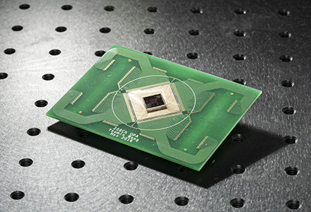
Because the researchers leverage mature CMOS technology, the basic component of all microprocessors, the device is programmable. This means that users can pre-program different hologram patterns on to the device. By stacking 160 x 160 fine-tuned polysilicon phase shifters on top of the MEMS actuators, the researchers were able to reduce beam divergence and increase the number of resolvable spots. This allows the device to achieve a large field-of-view and build a high-resolution 3D hologram of its surroundings. And, by using existing fabrication processes, this chip can be manufactured at comparatively lower cost than optical phased arrays made of liquid crystal.
In their demonstration, the Berkeley researchers achieved a resonance frequency of 55 kilohertz that corresponded to a response time — or time it takes for the optical phased array to change one hologram pattern to another — of 5.7 microseconds, almost 1,000 times faster than a traditional optical phased array built on liquid crystal. With a large array of 25,600 pixels packed onto a chip that is 3.1 by 3.2 millimeters, the device can also capture very high-resolution images of its surroundings.
"Being able to program these chips allows us to go beyond scanning, we can program our arrays to be more like human eyes. This allows us to generate and perceive arbitrary patterns like our eyes do; we can track individual objects instead of just rotating scanning,” said Ming Wu, professor of electrical engineering and computer sciences and corresponding author on the paper.