Researchers Demonstrate New 3D Printing Technique for Quantum Sensors
Innovation may lead to novel applications in precision measurement, biological imaging and environmental monitoring
Quantum sensing is an emerging field that holds great promise, but building the crystal substrate for these nanoscale sensors has proved challenging. Now, Berkeley researchers have developed a novel fabrication method to structure quantum sensing particles into complex 3D configurations that can accurately detect changes in temperature and magnetic fields in microscopic environments.
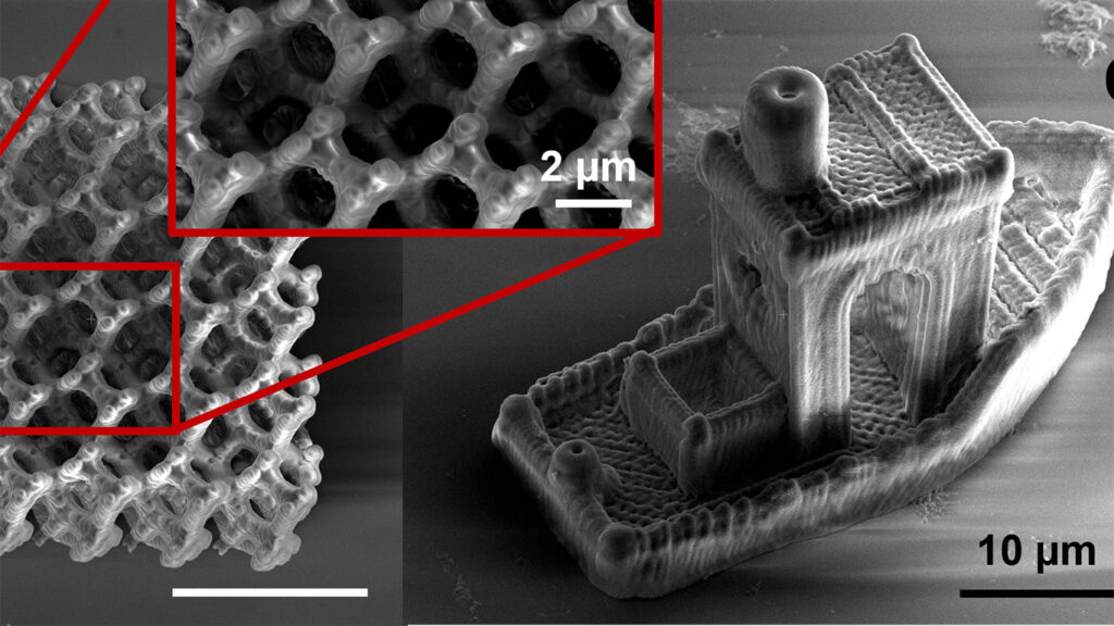
As reported in the journal Nano Letters, researchers used additive manufacturing methods to produce highly customizable 3D structures that can host tiny diamonds containing quantum sensing elements. These printable quantum sensors enable sensitive measurements at room temperature, which may open the door to transformative applications for materials science, biology and chemistry.
“Our work showcases the potential for integrating quantum sensors with advanced additive manufacturing techniques, which enable us to create new designs that are not otherwise possible,” said Brian Blankenship, co-lead author of the study and a graduate student in the Department of Mechanical Engineering. “In a couple of years, this technology might be used to incorporate sensors into microfluidics, electronics and biological systems — and open new avenues for the widespread utilization of quantum sensors for other applications that we haven’t even thought about yet.”
Co-principal investigator Costas Grigoropoulos, professor of mechanical engineering, added that because this new fabrication technique enables customization, structures can be precisely designed with the desired properties. “These architected materials are optimized to provide a tailored mechanical response,” said Grigoropoulos. “They combine sensing as well as actuation functionalities for applications in structural materials, tissue engineering and opto-mechanical systems.”
Quantum sensors use the properties of atoms and light to measure minute changes in magnetic and electric fields, strain and temperature. Today they are used in some of the most precise clocks on Earth that power GPS systems, and there is strong interest in applying these sensors in other areas, including neuroscience.
But taking quantum sensors out of pristine lab conditions is difficult, according to Grigoropoulos. “Many platforms for quantum sensing require extremely cold temperatures — hundreds of degrees below freezing — in order to function correctly,” he said. “In addition, these materials often need to be very clean and perfectly crystalline, which can prohibit their use in many practical applications.”
To tackle this problem, the researchers employed additive manufacturing techniques to structure quantum sensing particles, known as nitrogen vacancy centers, into 3D configurations. These nitrogen vacancy centers occur when a single carbon atom inside diamond is replaced by a nitrogen atom, and an adjacent carbon atom is empty. Nitrogen vacancy centers are unique because they work surprisingly well at room temperature and keep their quantum properties even when they are particles.
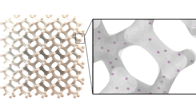
“Our approach overcomes the challenges associated with structuring single-crystal substrates, and these nitrogen vacancy centers can work reliably at room temperature,” said Blankenship. “We demonstrated that by using a modified microscope, we could take precise measurements of temperature and magnetic field measurements inside of these structures.”
According to Blankenship, the researchers are optimistic that this advancement will pave the way to new possibilities for quantum sensing.
“This technique now gives us the ability to print sensing elements into existing microfluidic chips, on top of advanced semiconductor devices and even cellular scaffolding, while providing advanced diagnostics for these systems,” he said. “And though our paper focuses on measuring temperature and magnetic fields, we believe this work can be extended to take other types of measurements as well.”
Grigoropoulos and Ashok Ajoy, assistant professor of chemistry, served as co-principal investigators of the study. Co-lead authors include Blankenship and Zachary Jones, a postdoctoral researcher in Ajoy’s lab and at Lawrence Berkeley National Laboratory. Co-authors are Naichen Zhao, Runxuan Li, Erin Suh and Alan Chen, all from the Department of Mechanical Engineering, and Harpreet Singh and Adrisha Sarkar from the Department of Chemistry.
Work done at the Laser Thermal Laboratory, a research group affiliated with the Department of Mechanical Engineering , is funded by the National Science Foundation. The lab’s main objective for this project was to design and fabricate complex hybrid materials using multiphoton lithography.