Jie Yao
Materials Science and EngineeringJie Yao is an Assistant Professor in the Department of Materials Science and Engineering. His research includes the study of novel optical materials and their applications in nanophotonics. He received his BS/MS degrees from Nanjing University, China and PhD in Applied Science and Technology from UC Berkeley.
Spark Award Project
Reconfigurable Photonics for the Next Generation Consumer Optics: Making Cameras Smarter and More Compact
Today conventional lenses are still used in smart phones, microscopes and many other devices. They are bulky and can only achieve a fixed functionality. With reconfigurable photonic devices, multiple functionalities can be achieved in one “smart lens”. One can choose from the functionalities which one to use. Moreover, such lenses are going to be much more compact than their conventional counterparts.
Jie Yao’s Story
As cell phones have become smaller, so have their camera lenses. Phones thinner than a cut deck of cards now capture images so sharp that they can be blown up beyond movie-poster size.
But the camera’s convex lenses impose an inherent limit on how thin the phone can be. With more than a billion-plus cell phones bought last year, manufacturers faced an unwelcome choice: either make a thicker camera or sacrifice the quality of the photos.
Now, another type of lens may be emerging, one with light-focusing power that does away with the classic convex piece of glass or plastic. Instead, it relies on “metamaterials” — fabricated arrays of nano-structures so named because they perform unlike any other natural substances.
Metamaterials are made of millions of nano-scale particles, each about the size of a virus. Although the particles themselves are made of atoms, their novel effects on material’s performance have earned them the name “artificial atoms.”
Materials scientist Jie Yao is developing a technique to fabricate one such metamaterial into a new form with strong commercial potential. He can transform a natural phase change material in a way that seems like alchemy, turning some sections of the material into metal but leaving others unchanged.
The metallic portions can interact with light as if they were nanoscale antennas, and Yao has shown that in certain conformations, the combined effect of tens of thousands of these antennas can focus light like a lens.
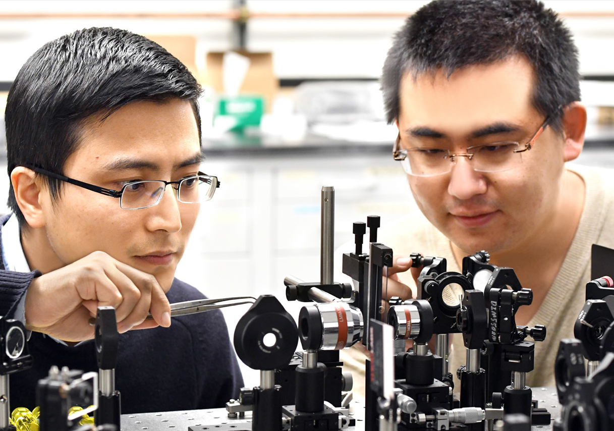
With support from the Bakar Fellows Program, his lab in the materials science and engineering department is fabricating nano-thin sheets of phase change material. The material is glass-like at room temperature but becomes metallic when heated slightly. Using a local heat source, Yao is able to convert part of the thin sheets into the metal antennas while letting other parts remain transparent.
The interactions of the nano-antennas with light are so effective that films hundreds of times thinner than a conventional lens could tightly control the path of light that passes through the film, Yao says.
He intends to refine his technology’s novel ability to tweak the metallic components’ 3-D shape, and he hopes to open up a range of applications to control visible light as well as infrared and microwave wavelengths.
“The metallic phase change material is the working part of the material, while the insulating part provides the matrix to hold the ‘artificial atoms’ in place,” Yao says.
“When a broad beam of light hits the array, it can be considered as composed of many finer beams. Each new beam passes by an antenna, which is able to change its unique path.
“Using a local heat source, we can ‘write’ new structures into the material. Then, by lowering the temperature, we can erase and re-write them. We can change the material’s structure, and performance at will. No complicated nano-fabrication process is needed.”
By using this etch-a-sketch local heating strategy, his team can change the material’s configuration in real time — potentially in less than a second. “In this we may be able to create a dynamic optical device, for example, a single lens whose focus can be changed whenever necessary,” Yao says.
The array can be “written” in such a way that each antenna will guide light to the same focal point to form a lens. The next moment, the array can be erased and a new array may be written, and the focal point changed to another location, which could be used to improve the performance of photography and other imaging processes.
Beyond the vision of new lenses for a billion cell phones, the technology’s ability to control visible light could yield-thin computer or wall displays. In principle, Yao says, the material and the transforming technique can yield conformations to manipulate infrared light, or microwave radiation as well, leading to novel types of infrared sensors and other optical devices.
“The material is a platform that allows us to draw any photonic structure, so we really can achieve a range of applications and transform them from static devices to dynamic ones.”