Research Expertise and Interest
nanotechnology, low power electronics, flexible electronics and sensors, nanofabrication, energy harvesting and conversion, programmable matter
Research Description
Ali Javey is the Lam Research Distinguished Chair in Semiconductor Processing and a professor of Electrical Engineering and Computer Sciences. The core of Javey’s research program is materials innovation for enabling new device structures and concepts. The lab studies a wide range of electronic materials in both planar and 3D geometries. In all cases, the lab explores new schemes of manipulating, processing, and engineering materials - often at unprecedented levels - to enable new functionalities and properties. Below are some research highlights.
- Developed a new doping technology named monolayer doping (MLD) that utilizes surface chemistry to form self-assembled monolayers of dopant containing species on semiconductor surfaces followed by a subsequent diffusion by a thermal annealing (Nature Materials, 2008). The process has yielded some of the shallowest junctions reported to date, down to ~3 nm in thickness. The technology has been transferred to the semiconductor industry for further internal R&D, and is seen as a promising approach for S/D contact extensions for future nanoscale transistors.
- Developed the ultrathin body III-V on insulator (XOI) device concept as a platform for integrating high mobility III-V semiconductors on Si for low power electronics (Nature, 2010). Reported p- and n-type III-V FETs with some of the highest mobilities reported to-date on a Si substrate with a subthreshold swing as low as ~70 mV/decade, approaching the ideal limit of MOSFETs.
- Discovered the quantum unit of absorptance in 2D semiconductors (in collaboration with E. Yablonovitch; PNAS, 2013).
- Developed a new growth mode for III-V thin films using the vapor-liquid-solid (VLS) technique (Scientific Reports, 2013). As a proof of concept, InP thin films (on the order of 1µm in thickness) are grown on non-epitaxial substrates (e.g., metal foils) using the thin-film VLS process with an ultralarge grain size of up to ~ 1mm and optoelectronic properties (including luminescence yield) approaching those of epitaxially grown layers. The work presents a promising route for low-cost growth of high quality III-V semiconductors for PV applications and beyond.
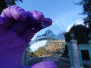
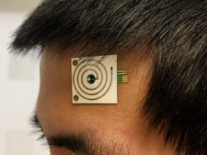
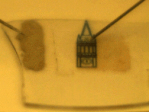
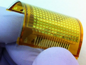
- Developed process techniques for uniform assembly of nanostructured materials (e.g., nanowires and nanotubes) over large-areas for system integration – moving beyond individual device work (Nature Materials, 2013; Nature Materials, 2010). As a proof of concept, Javey’s lab has demonstrated large-area monolithic integration of nanotube TFTs, pressure sensors, and OLEDs on a plastic substrate that can map pressure and provide instantaneous visual response through the integrated OLED display. The work presents a platform for 3-D integration of different material/device components for paper-thin smart/interactive surfaces, and is an elegant example of systems enabled by nanomanufacturing.